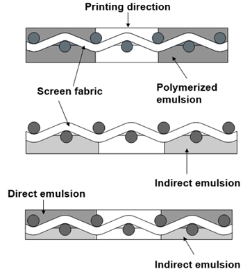
Schematic screen printing thick film setup.
By A Mystery Man Writer
Description
MECA courses - Home

Step by Step to Explain Printed Circuit Board (PCB) Manufacturing
Dynamic X-ray imaging with screen-printed perovskite CMOS array

a) SEM image and (b) EDS spectra of TiO2 screen printed film

Aslam KHAN, Professor (Assistant), PhD

The basic screen-printing process
PDF) Screen printed TiO2 film: A candidate for photovoltaic
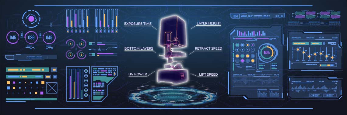
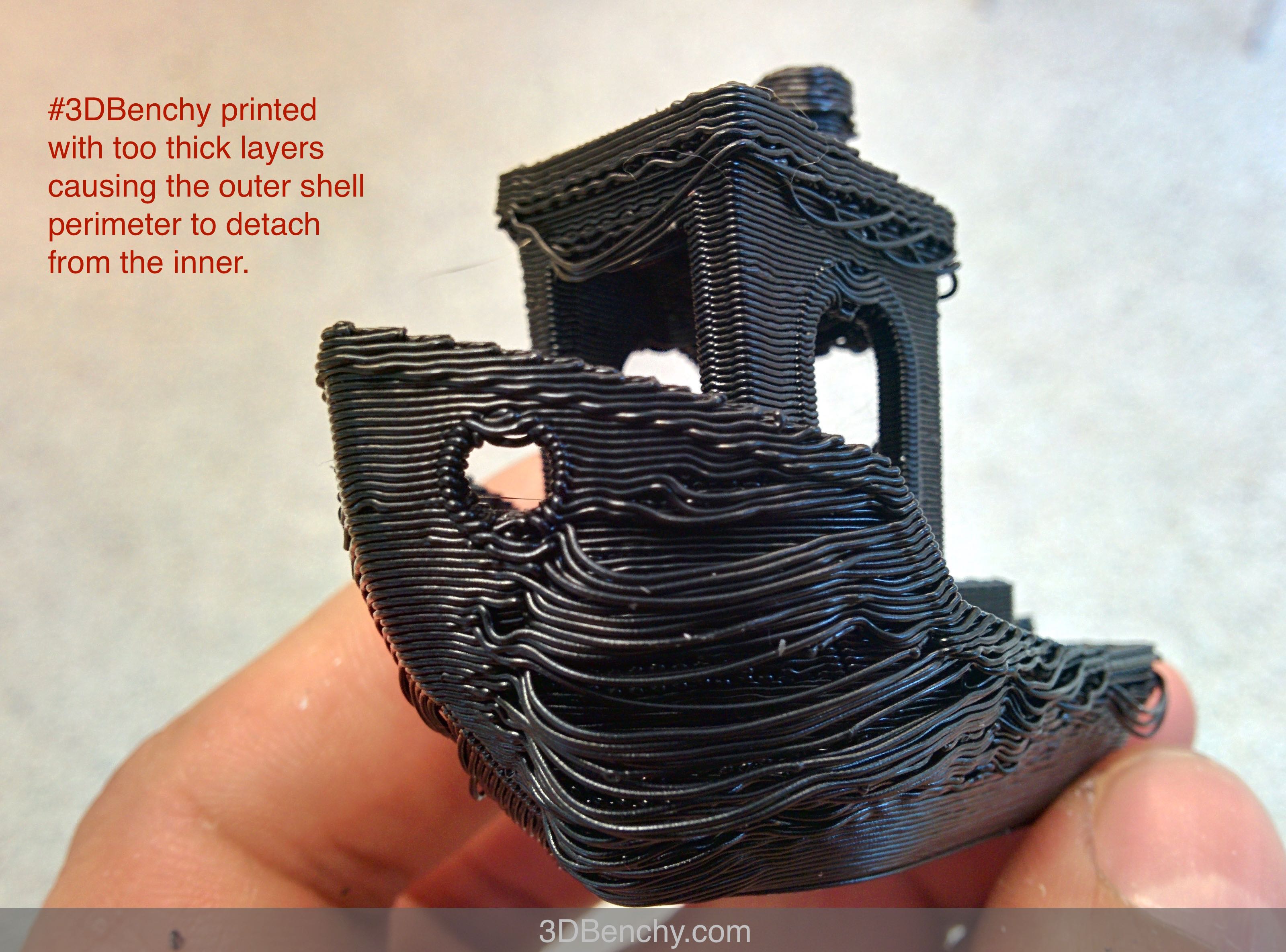
The Complete Resin 3D Printing Settings Guide for Beginners

Screen Printing Imprint Placement Guide
from
per adult (price varies by group size)